Plastic Fabrications
CBM2 Plastics Engineering for Microfluidics and Nanofluidics
CBM2 has been involved in building and using polymer-based microfluidic systems since 1995 for a variety of biomedical applications. We have generated a significant amount of know-how and infrastructure to develop and design highly innovative devices. CBM2’s multi-institutional format, with resources available at Center-associated infrastructure situated at KU-L, UNC, and LSU, facilitates innovation. We recently expanded our already extensive resources for building and using nanofluidic devices using plastics as the substrate material. This is a very unique capability of CBM2. We have the necessary tools to build even sub-10 nm structures in plastics. Structures can be sealed with cover plates with high process yield rates. Our team has know-how in terms of assembly and functionalization of devices. CBM2 possesses unique fabrication tools across many length scales: Rapid Prototyping, Micro- and nanofabrication of molding tools, Replication, and Metrology. Selected applications of our devices for various biomedical applications. Micro- and nanofabrication infrastructure. Our plastic fabrication infrastructure is located at three sites as noted above and possesses tools for rapid prototyping, microfabrication, nanofabrication, and metrology.
Micro- and nanofabrication infrastructure
Our plastic fabrication infrastructure is located at three sites as noted above and possesses tools for rapid prototyping, microfabrication, nanofabrication, and metrology.
Rapid Prototyping
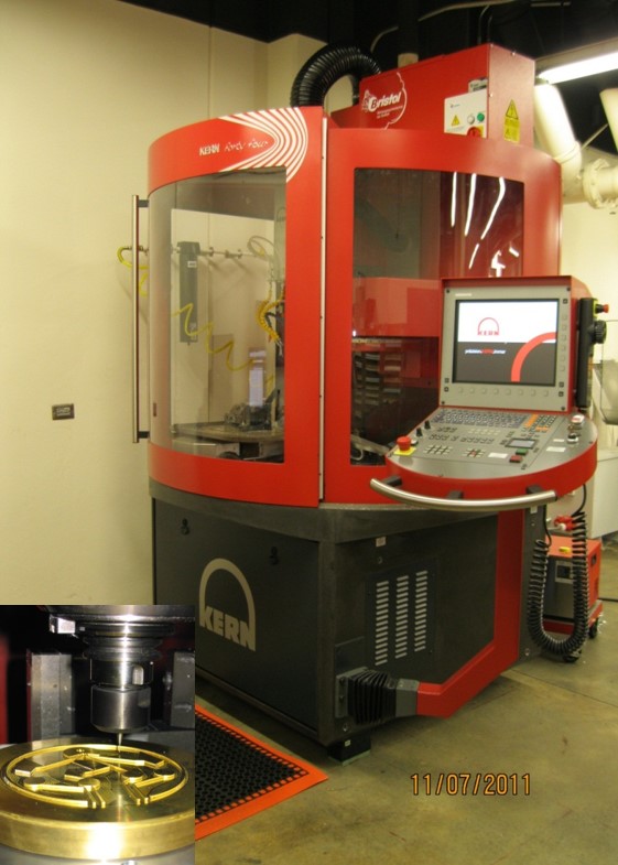
We have two machines to do rapid prototyping of microfluidic devices in plastics. These include a high precision micromill (KU, LSU, and UNC) and a laser milling system using both an excimer laser (UNC) and a CO2 laser (KU). The milling machine can spin carbide bits as small as 25 µm by spinning at extremely high revolution rates. The mill can be used to write structures directly into plastics or into soft metals such as brass, which can be subsequently used a molding tools for hot embossing or injection molding. Channel widths as small as 25 µm can be fabricated with aspect ratios of 4:1 and side wall roughness ~300 nm.
Micro/nanofabrication (replication):
We have developed world-class fabrication (replication) capabilities of plastic devices using a variety of techniques such as hot embossing, imprinting, nanoimprint lithography (NIL), and injection molding (also injection compression molding). In addition, we have great working relationships with several commercial foundries such as Stratec.
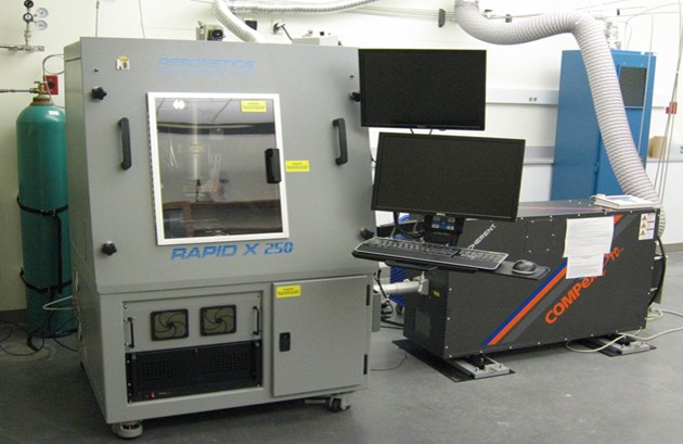
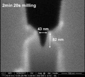
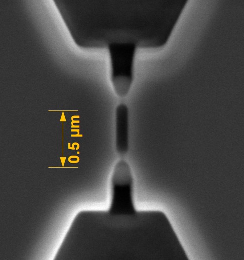
Typically replication-based technologies, no matter what the scale (micro or nano), require molding tools, and CBM2 has a variety of methods it has perfected to build masters for replication production of final devices. For example, we can make molding tools for hot embossing and injection molding using high precision Micromilling, and if feature sizes demand (<10 µm with aspect ratios >5:1), we can use a combination of lithography and electroplating (LiGA) to build the desired molding tools. For nanoscale structures, we use the nano-patterning capabilities we have access to, which consists of focused ion beam milling to make nanostructures and conventional optical lithography to build microstructures. This is followed by using UV-NIL to make resin stamps that can go into our NIL machines to produce final parts in plastics via thermal NIL. The Center is fortified by the extensive resources found in our cleanrooms, such as KUNF at the University of Kansas, CHANL at the University of North Carolina, and CAMD at Louisiana State University.
Here are the replication tools we possess within the Center:
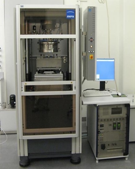
- Jenoptik HEX02 (LSU) and HEX03 (KU and UNC)
- PHI Precision Press (KU)
- Wabash Press (KU)
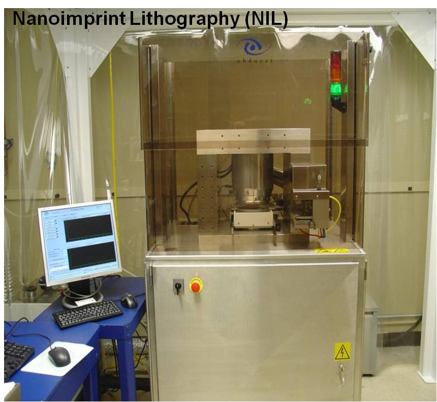
- Obducat NIL machine (LSU)
- Nanonex NIL machine (KU)
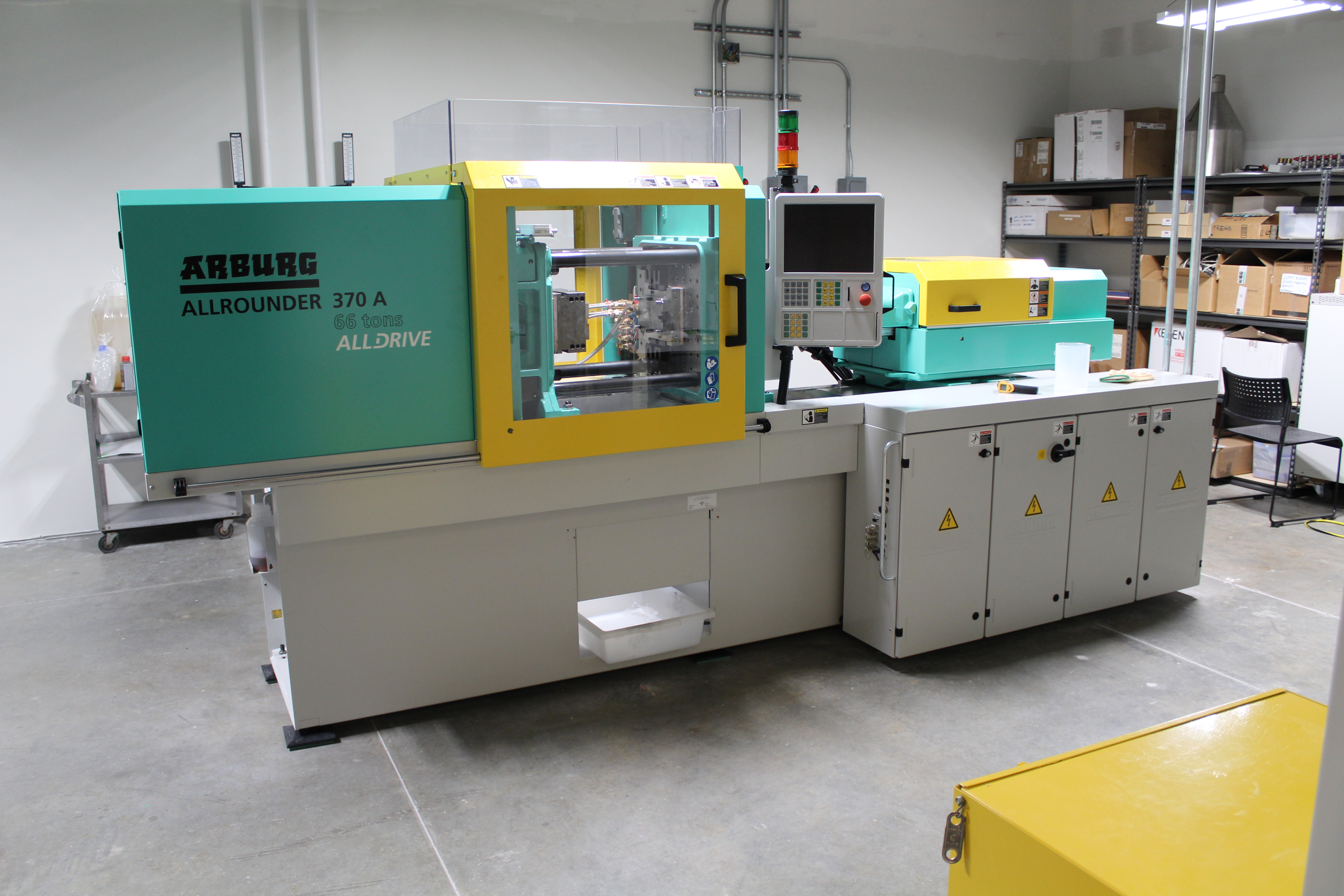
- Arburg injection molding machine (also does injection compression molding) (KU)
Metrology
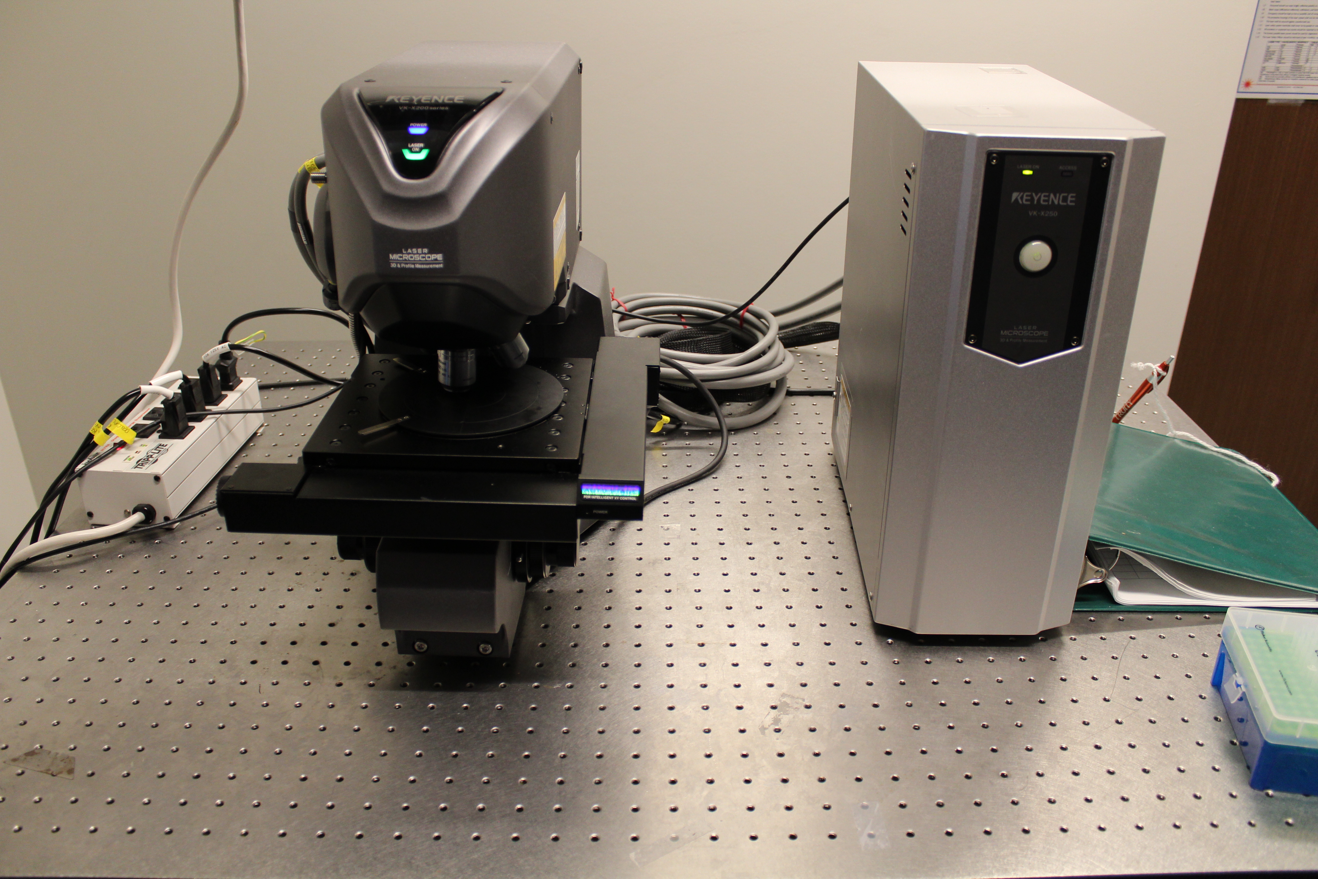
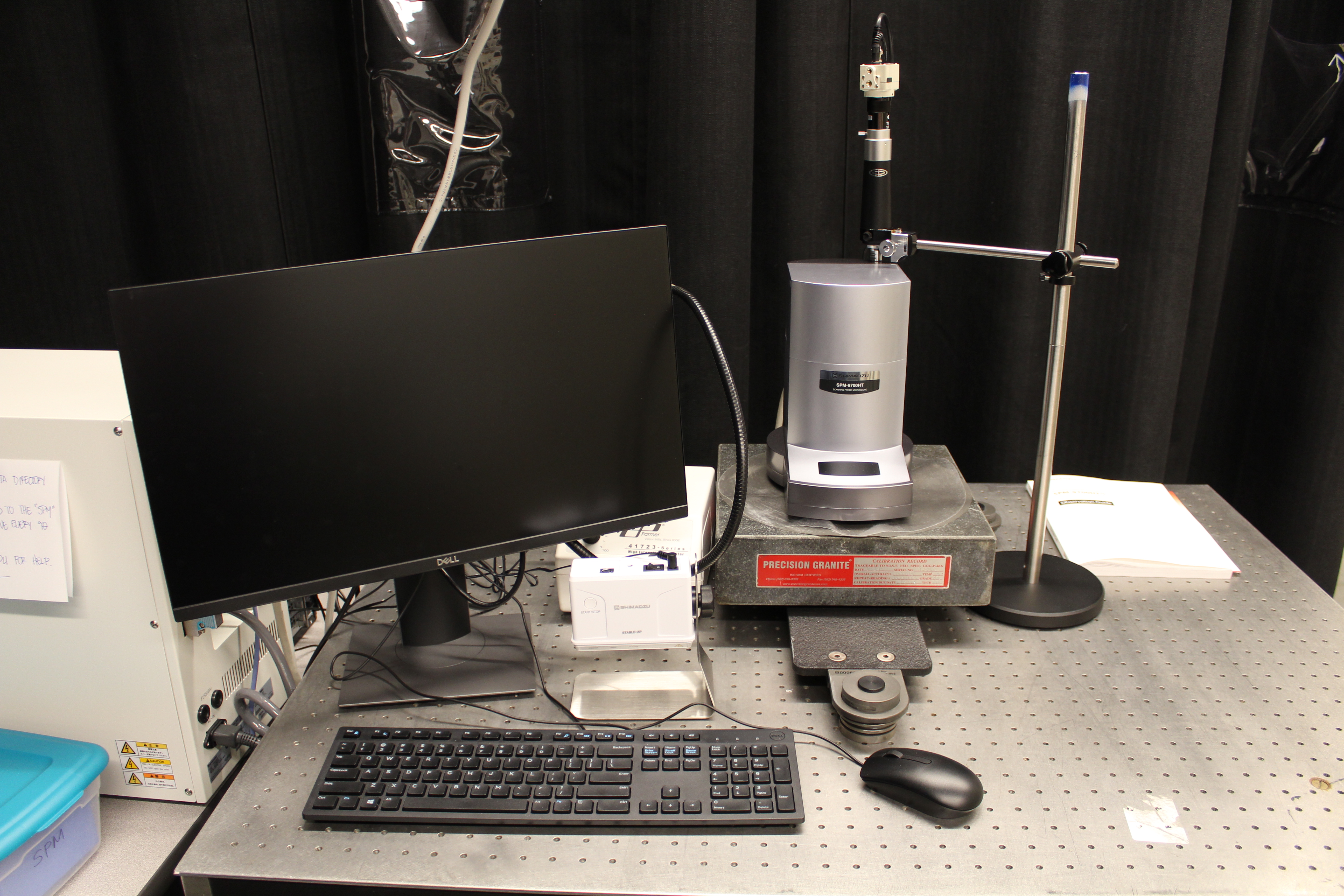
We have within the Center, several tools for metrology across many different length scales. For example, we have several AFMs for determining replication fidelity in nanofluidic devices including a new Shimadzu scanning probe microscope and a Keyence rapid scanning confocal microscope for performing non-contact profilometry. The Keyence uses a violet laser that allows for depth profiling around 100 nm.
Device assembly and functionalization
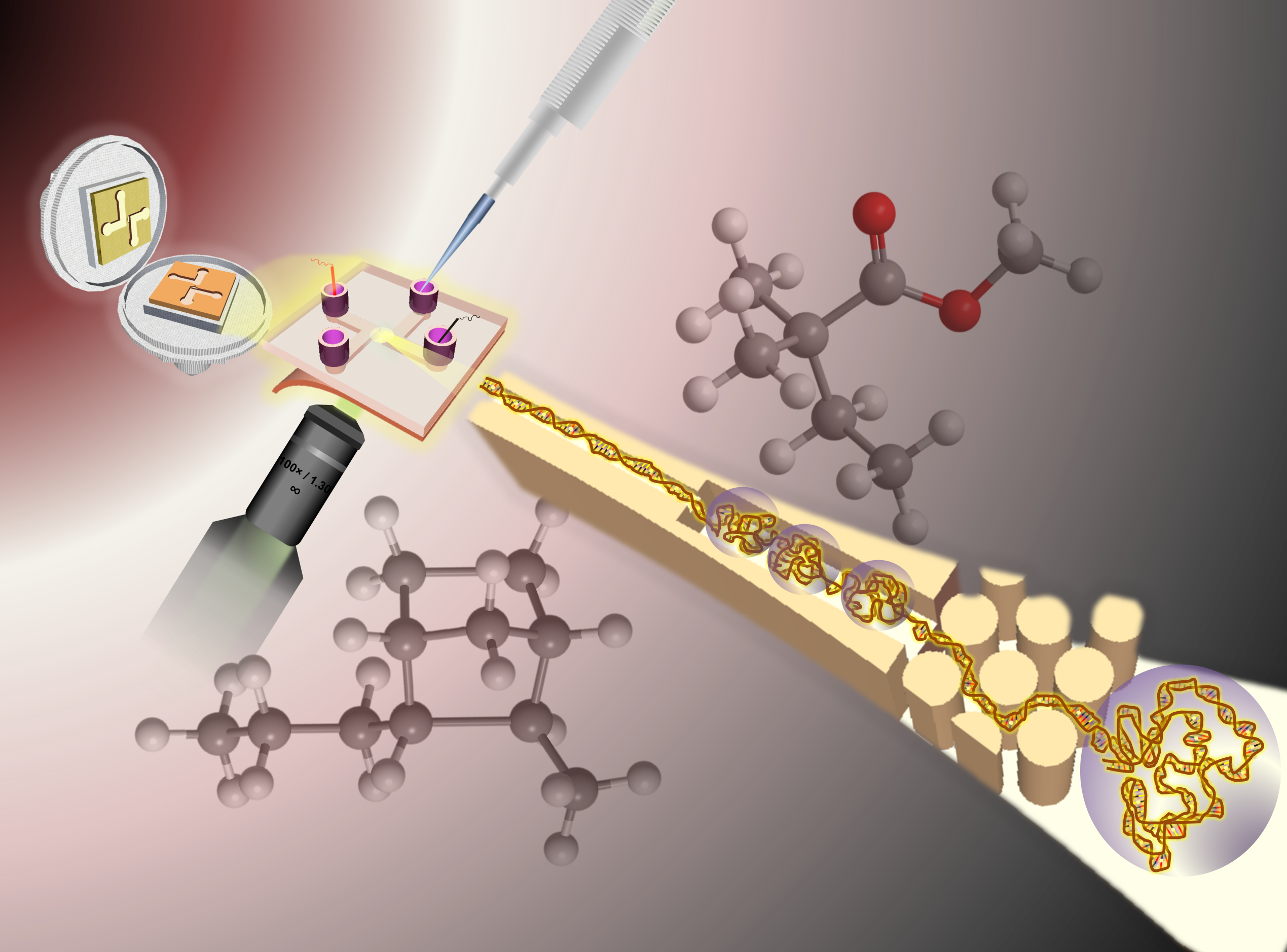
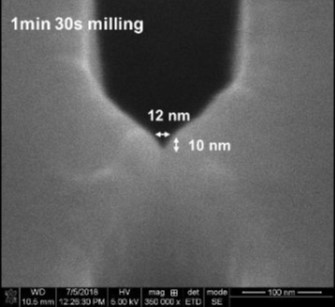
In the case of nanofluidic devices, we use a hybrid-based approach, which consists of thermal fusion bonding a high Tg substrate to a low Tg cover plate. When using bonding temperature close to the Tg of the cover plate, we can generate process yield rates >90% even for devices containing nanostructures as small as 10 nm.
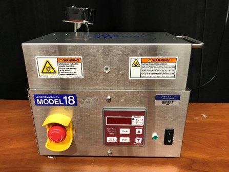
Following device assembly, we can activate the surface of the plastic to both make it more hydrophilic (i.e., wettable) and create functional scaffolds (surface-confined carboxylic acids) for the covalent attachment of biologics, such as recognition elements or enzymes, using standard EDC/NHS coupling chemistry. This can be accomplished by exposing the device to UV/O3 radiation using a very simple instrument.
Applications of plastic devices
We have placed in the public domain a number of publications that highlight our ability to not only fabricate microfluidic and nanofluidic devices, but also use them in compelling biomedical applications. For example, we have used our plastic-based microfluidic devices for ultra-fast PCRs, electrophoresis, electrochromatography, solid-phase extractions, ligase detection reactions for the detection of point mutations, micro-optics, solid-phase bioreactors, and the isolation of liquid biopsy markers.
In terms of nanofluidics, which is a relatively new area for us, we have leveraged our ability to build functional devices with sub-100 nm structures for such applications of electrophoresis analysis of both small and large molecules, stretching DNA to detect chemotherapy-induced damage, and a new application we are developing which involves a single-molecule DNA/RNA sequencing platform (being co-developed by our commercial partner, Sunflower Genomics, Inc.).
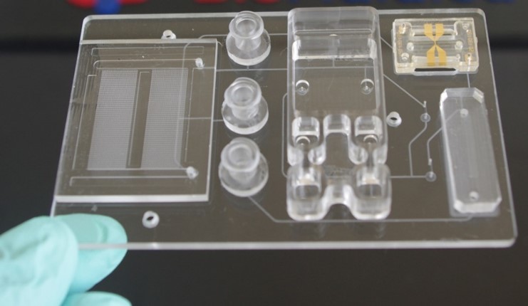
We have also used many of the discoveries emanating from the Center to develop integrated and modular mixed-scale systems that can perform multi-step assays in a fully automated fashion. The integrated system idea we are pursuing is a modular one, in which task-specific modules are connected to a fluidic motherboard. The connections of the modules to the motherboard is achieved using superhydrophobic seals. The modules can be used as standalone units as well. We are adopting a universal fluidic motherboard approach so that modules can be easily interchanged to change the function of the system.